- 您现在的位置:买卖IC网 > Sheet目录330 > IDT71V124SA10PHGI (IDT, Integrated Device Technology Inc)IC SRAM 1MBIT 10NS 32TSOP
IDT71V124SA, 3.3V CMOS Static RAM
1 Meg (128K x 8-Bit) Center Power & Ground Pinout
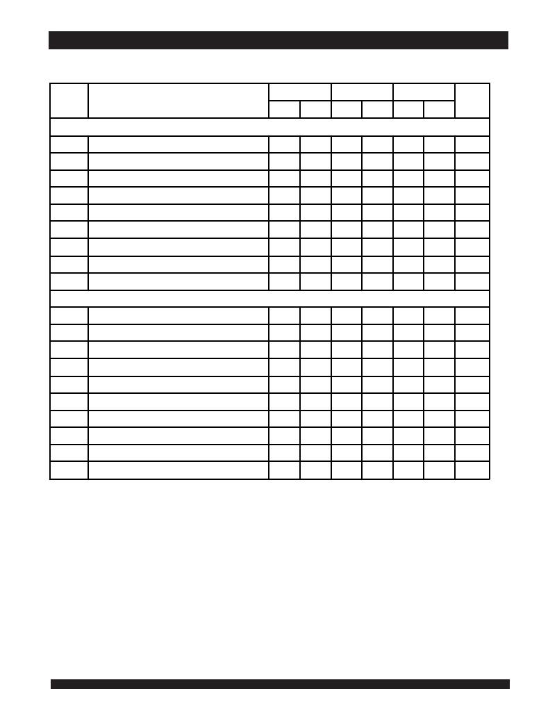
Commercial and Industrial Temperature Ranges
AC Electrical Characteristics
(V DD = Min. to Max., Commercial and Industrial Temperature Ranges)
71V124SA10
71V124SA12
71V124SA15
Symbol
Parameter
Min.
Max.
Min.
Max.
Min.
Max.
Unit
READ CYCLE
t OLZ
t RC
t AA
t ACS
t CLZ (1)
t CHZ (1)
t OE
(1)
t OHZ (1)
t OH
Read Cycle Time
Address Access Time
Chip Select Access Time
Chip Select to Output in Low-Z
Chip Deselect to Output in High-Z
Output Enable to Output Valid
Output Enable to Output in Low-Z
Output Disable to Output in High-Z
Output Hold from Address Change
10
____
____
4
0
____
0
0
4
____
10
10
____
5
5
____
5
____
12
____
____
4
0
____
0
0
4
____
12
12
____
6
6
____
5
____
15
____
____
4
0
____
0
0
4
____
15
15
____
7
7
____
5
____
ns
ns
ns
ns
ns
ns
ns
ns
ns
WRITE CYCLE
t WC
t AW
t CW
t AS
t WP
t WR
t DW
t DH
t OW (2)
t WHZ (2)
Write Cycle Time
Address Valid to End-of-Write
Chip Select to End-of-Write
Address Set-up Time
Write Pulse Width
Write Recovery Time
Data Valid to End-of-Write
Data Hold Time
Output Active from End-of-Write
Write Enable to Output in High-Z
10
7
7
0
7
0
5
0
3
0
____
____
____
____
____
____
____
____
____
5
12
8
8
0
8
0
6
0
3
0
____
____
____
____
____
____
____
____
____
5
15
10
10
0
10
0
7
0
3
0
____
____
____
____
____
____
____
____
____
5
ns
ns
ns
ns
ns
ns
ns
ns
ns
ns
NOTES:
1. This parameter guaranteed with the AC load (Figure 2) by device characterization, but is not production tested.
4
3873 tbl 08
发布紧急采购,3分钟左右您将得到回复。
相关PDF资料
IDT71V256SA20PZG
IC SRAM 256KBIT 20NS 28TSOP
IDT71V25761S200PFGI
IC SRAM 4MBIT 200MHZ 100TQFP
IDT71V30L35TFI
IC SRAM 8KBIT 35NS 64STQFP
IDT71V321L25TFI
IC SRAM 16KBIT 25NS 64STQFP
IDT71V3556SA166BGGI
IC SRAM 4MBIT 166MHZ 119BGA
IDT71V3559S85BQI
IC SRAM 4MBIT 85NS 165FBGA
IDT71V35761YSA200BGI
IC SRAM 4MBIT 200MHZ 119BGA
IDT71V3577S75BQG
IC SRAM 4MBIT 75NS 165FBGA
相关代理商/技术参数
IDT71V124SA10PHGI8
功能描述:IC SRAM 1MBIT 10NS 32TSOP RoHS:是 类别:集成电路 (IC) >> 存储器 系列:- 标准包装:72 系列:- 格式 - 存储器:RAM 存储器类型:SRAM - 同步 存储容量:4.5M(256K x 18) 速度:133MHz 接口:并联 电源电压:3.135 V ~ 3.465 V 工作温度:0°C ~ 70°C 封装/外壳:100-LQFP 供应商设备封装:100-TQFP(14x20) 包装:托盘
IDT71V124SA10TY
功能描述:IC SRAM 1MBIT 10NS 32SOJ RoHS:否 类别:集成电路 (IC) >> 存储器 系列:- 产品变化通告:Product Discontinuation 05/Nov/2008 标准包装:84 系列:- 格式 - 存储器:RAM 存储器类型:SRAM - 同步 ZBT 存储容量:4.5M(128K x 36) 速度:75ns 接口:并联 电源电压:3.135 V ~ 3.465 V 工作温度:-40°C ~ 85°C 封装/外壳:119-BGA 供应商设备封装:119-PBGA(14x22) 包装:托盘 其它名称:71V3557SA75BGI
IDT71V124SA10TY8
功能描述:IC SRAM 1MBIT 10NS 32SOJ RoHS:否 类别:集成电路 (IC) >> 存储器 系列:- 产品变化通告:Product Discontinuation 05/Nov/2008 标准包装:84 系列:- 格式 - 存储器:RAM 存储器类型:SRAM - 同步 ZBT 存储容量:4.5M(128K x 36) 速度:75ns 接口:并联 电源电压:3.135 V ~ 3.465 V 工作温度:-40°C ~ 85°C 封装/外壳:119-BGA 供应商设备封装:119-PBGA(14x22) 包装:托盘 其它名称:71V3557SA75BGI
IDT71V124SA10TYG
功能描述:IC SRAM 1MBIT 10NS 32SOJ RoHS:是 类别:集成电路 (IC) >> 存储器 系列:- 标准包装:2,000 系列:- 格式 - 存储器:RAM 存储器类型:SRAM - 异步 存储容量:256K (32K x 8) 速度:15ns 接口:并联 电源电压:3 V ~ 3.6 V 工作温度:-40°C ~ 85°C 封装/外壳:28-TSSOP(0.465",11.8mm 宽) 供应商设备封装:28-TSOP 包装:带卷 (TR) 其它名称:71V256SA15PZGI8
IDT71V124SA10TYG8
功能描述:IC SRAM 1MBIT 10NS 32SOJ RoHS:是 类别:集成电路 (IC) >> 存储器 系列:- 标准包装:2,000 系列:- 格式 - 存储器:RAM 存储器类型:SRAM - 异步 存储容量:256K (32K x 8) 速度:15ns 接口:并联 电源电压:3 V ~ 3.6 V 工作温度:-40°C ~ 85°C 封装/外壳:28-TSSOP(0.465",11.8mm 宽) 供应商设备封装:28-TSOP 包装:带卷 (TR) 其它名称:71V256SA15PZGI8
IDT71V124SA10TYGI
功能描述:IC SRAM 1MBIT 10NS 32SOJ RoHS:是 类别:集成电路 (IC) >> 存储器 系列:- 产品变化通告:Product Discontinuation 05/Nov/2008 标准包装:84 系列:- 格式 - 存储器:RAM 存储器类型:SRAM - 同步 ZBT 存储容量:4.5M(128K x 36) 速度:75ns 接口:并联 电源电压:3.135 V ~ 3.465 V 工作温度:-40°C ~ 85°C 封装/外壳:119-BGA 供应商设备封装:119-PBGA(14x22) 包装:托盘 其它名称:71V3557SA75BGI
IDT71V124SA10TYGI8
功能描述:IC SRAM 1MBIT 10NS 32SOJ RoHS:是 类别:集成电路 (IC) >> 存储器 系列:- 产品变化通告:Product Discontinuation 05/Nov/2008 标准包装:84 系列:- 格式 - 存储器:RAM 存储器类型:SRAM - 同步 ZBT 存储容量:4.5M(128K x 36) 速度:75ns 接口:并联 电源电压:3.135 V ~ 3.465 V 工作温度:-40°C ~ 85°C 封装/外壳:119-BGA 供应商设备封装:119-PBGA(14x22) 包装:托盘 其它名称:71V3557SA75BGI
IDT71V124SA10Y
功能描述:IC SRAM 1MBIT 10NS 32SOJ RoHS:否 类别:集成电路 (IC) >> 存储器 系列:- 产品变化通告:Product Discontinuation 05/Nov/2008 标准包装:84 系列:- 格式 - 存储器:RAM 存储器类型:SRAM - 同步 ZBT 存储容量:4.5M(128K x 36) 速度:75ns 接口:并联 电源电压:3.135 V ~ 3.465 V 工作温度:-40°C ~ 85°C 封装/外壳:119-BGA 供应商设备封装:119-PBGA(14x22) 包装:托盘 其它名称:71V3557SA75BGI
